ABOUT US
GREETING
Catalog
ABOUT NAS Giken
-
The Highest Quality of Bulk Etching Function
Our bulk etching function can allow etching process of the entire surface of the wafer to recover contaminants inside the wafer. When performing bulk etching, the "flatness" that determines whether the surface can be dug evenly is one of the most important factors. Our etching performance can guarantee flatness within 10% and have satisfied various customers up to now.
-
World-class Wafers Contamination Recovery System
We have obtained an international patent for "bevel recovery," which is a contamination recovery operation on the side of a silicon wafer. Also, we have granted a domestic patent regarding to the sampling of the hydrophilic wafer surface. Our technology stands for uncompromising quality and precision all over the world.
-
Perfect After-Sales Service
We provide maintenance service both all over Japan also overseas customers. Our sales support shall respond to customer inquiries from Japan in within 24 hours (overseas less than 48 hours). When confirming maintenance details, we may visit your site, hold telephone or online conferences with as appropriate.
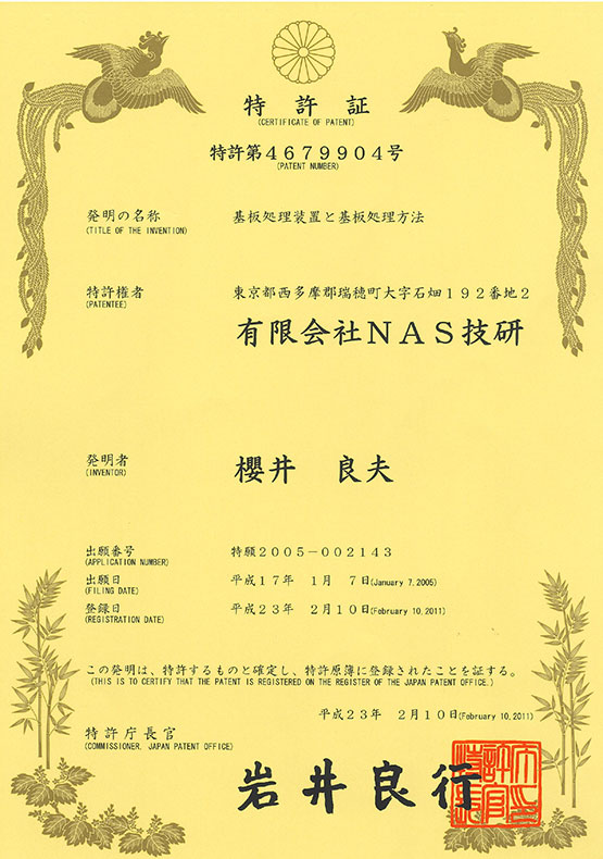
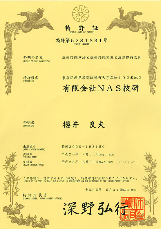
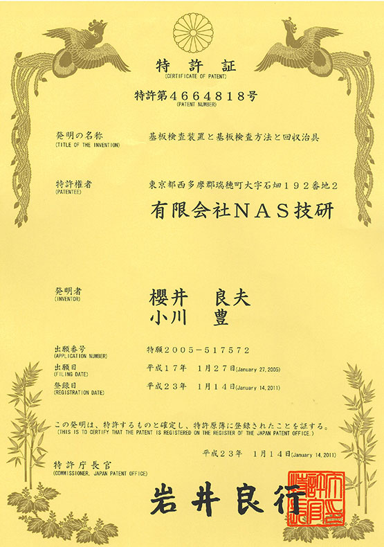
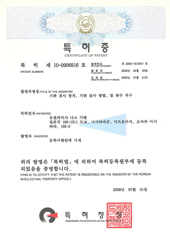
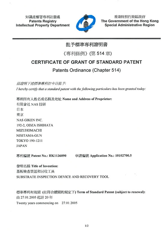
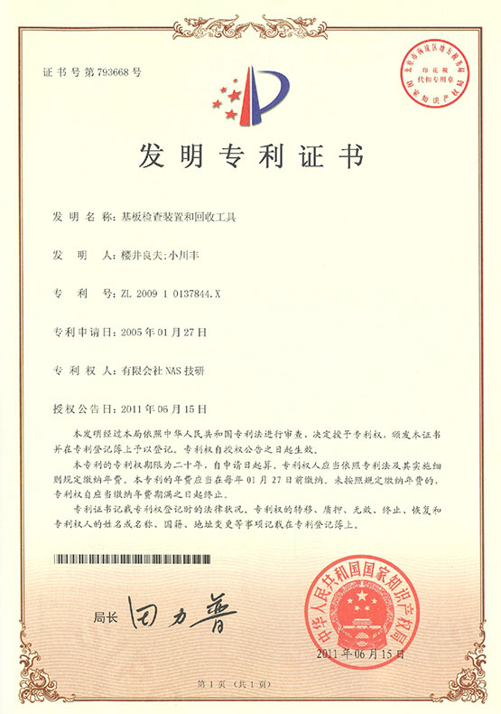
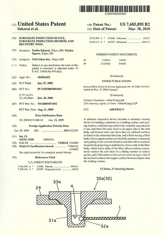
PATENT
COMPANY PROFILE
| Company Name | NAS Giken, Inc. |
|---|---|
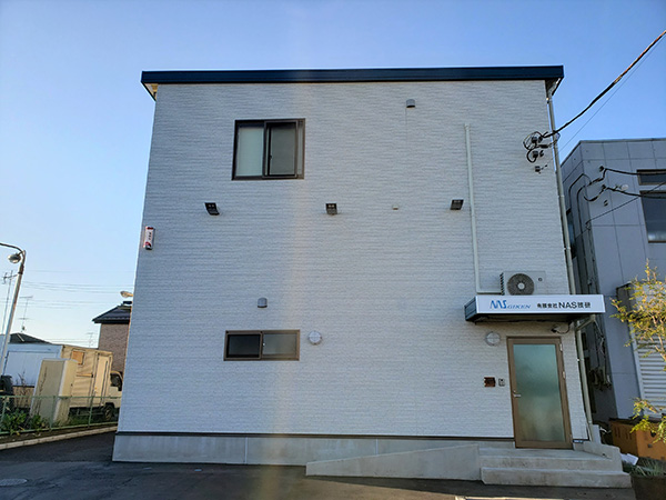
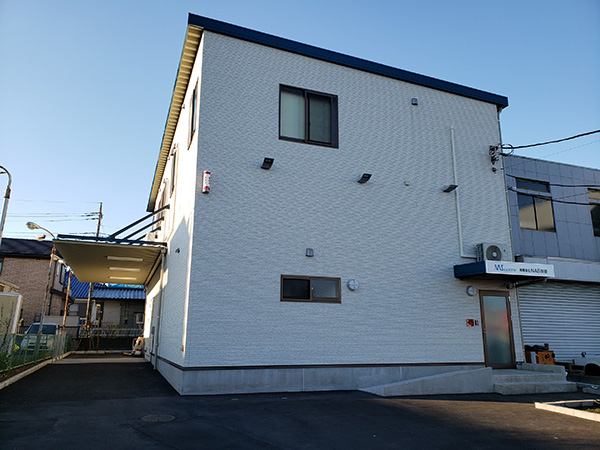
| Headquarters | 36-7 Higashimatsubara, Hakonegasaki, Mizuho-machi,Nishitama-gun, Tokyo 190-1222 |
| Founded | 25, October, 2002 |
| Share Capital | 3,000,000 JPY |
| Business | Manufacture devices of both sampling metal contamination on surface & bevels of wafers and bulk etching. |
| Number of Employees | 10 (Permanent) |
| Customers | Major Wafers manufacturers, device and analysis companies in the semiconductor industry. |
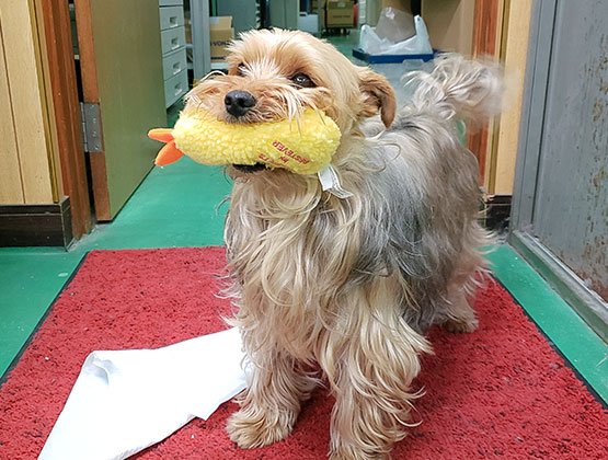
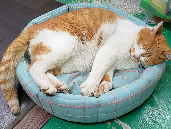
STAFF
LALA【♀】
・Working for 13 years
・She works as Customer Service in house Patrol
OCHOKO【♂】
・Working for 18 years
・He makes us feel relaxed at the office.
CONTACT US
Please complete the form and submit if you request a quote or product information.
A NAS Giken representative will contact you regarding your request.
Call to speak to us 9:00-17:00
(Monday to Friday)
Tel. +81-42-557-5207
![]()
Inquiry Form